
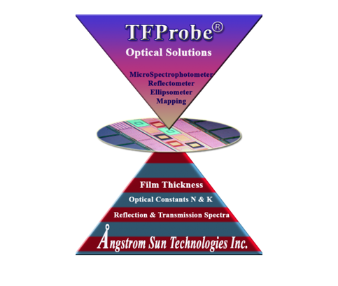
Angstrom Sun Technologies Inc., headquartered in Boston, USA, is a privately held company specializing in affordable optical solutions. Our focus is on providing cost-effective tools for characterizing various parameters such as thin film thickness, thick coating thickness, wafer thickness, gap thickness, optical properties (refractive index N and extinction coefficient K), surface behavior, interface behavior, alloy concentrations, and their uniformities across surfaces.
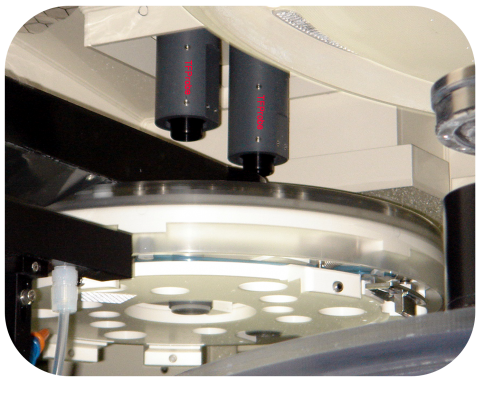
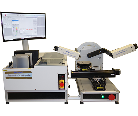
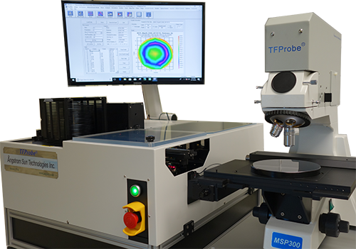
Our range of tools includes spectroscopic reflectometers, microspectrophotometers, microreflectometers, film thickness mapping systems, simple desktop film thickness stations, and automatic variable angle spectroscopic ellipsometers, as well as wafer and gap thickness tools. These tools are designed to offer advanced and high-performance capabilities at a low cost, allowing nondestructive and precise probing of film stacks and wafers. Additionally, we provide advanced analytical services for characterizing thin films, thick coatings, complex layer stacks, wafer thickness, TTV (Total Thickness Variation), and gap thickness. We also offer various vision products with USB directshow, USB3 vision, GigE, and GenTL compatible cameras.
With performance and professional support as our mission, Angstrom has established a worldwide customer base since 2002, including well-known education institutions, government agencies and Fortune 500 companies, such as NASA Marshall Space Flight Center, National Institute of Standards and Technology, Massachusetts Institute of Technology (MIT), Seoul National University, NanoTech Center (CESTM) at SUNY, Columbia University, Hewlett-Packard Co., Lockheed Martin Co., General Electric (GE), Corning Inc., Bell Laboratories, Johnson-Johnson, Mylan Technologies, Applied Materials (AMAT), Lam Research, Samsung Advanced Institute of Technology(SAIT), UC Berkeley and MIT Lincoln Laboratory........
Both spectroscopic ellipsometry and reflectometry are model-based techniques, and we understand the importance of advanced software and professional application support in implementing these tools for various thin film applications. Therefore, we provide unlimited application modeling assistance and free software upgrades with our tools. Our focus is not just on selling our products but on ensuring that our customers can use our tools to achieve their desired outcomes.
Testimonials:
“We've recently purchased a basic version of TFProbe reflectometer from Angstrom Sun Technologies Inc. This instrument has the best price/functions ratio among all others we had a look at and it is totally suitable for our simple tasks. The setting up and learning how to run the instrument did not take long. In my opinion, it is much easier to run this tool, comparing to run thier competitor's tool I have used before. When I have plotted my first calibration curve for the film thickness vs amount deposited on Silicon wafer surface, I was pleasantly and surprised by the fact that linearity was R=0.99988! We would like to thank Professionials at Angstrom Sun tech for their kind assistance during process of choosing right instrument, its purchase and installation. Great product, very nice knowledgeable and highly professional people and services. “
----- By Dr. Tatiana Svitova, Senior research associate, CRC, School of Optometry, UC Berkeley
“We did a trade study of what we considered to be the seven-best spectroscopic ellipsometers that we could afford. We sent test films deposited on 150mm diameter Si wafers to each manufacturer to ascertain their tool meets our applications: (1) ~120nm of SiGe on ~100nm of SiO2 on Si; (2) ~120nm of TiN on ~1000nm of SiO2 on Si; (3) ~100nm of Ge on Si.
Only two companies correctly measured each index and each individual thickness respectively. Angstrom Sun Tech is one of them. We were interested in the visible and getting as far into the IR as possible without buying the IR version (out of our price range). We found that the Angstrom Sun Technology SE200BM spectrum went from 250nm – 1100nm. In addition to measuring films that allow the shorter visible wavelengths to pass, the longer wavelengths allowed us to characterize GaAs/AlGaAs quantum well structures, and a host of other patterned films such as Ge and Si that have high lost in the visible. Further, the motorized mapping allowed us to reliably measure uniformity. Finally, the bottom line – Angstrom Sun Tech came in at the lowest price.
It doesn’t stop there. After delivery, the Angstrom engineer constantly answered all of our questions to set up tool and in using the tool (we set it up by ourselves). They even come out to UC Berkeley Nanofabrication Laboratory to make sure that we were happy with our purchase, and to answer any lingering questions. The reason why we are very happy with the tool is because Angstrom stands behind the tool. We whole-heartedly recommend this tool to anyone who needs precision at a reasonable price.”
--- by Richelieu Hemphill, Marvell Nanofabrication Laboratory, University of California, Berkeley
“In R&D, we deposit, etch, and change films day in and day out. The support we have received from Angstrom Sun Tech has been exceptional. For the last 7 years we have been using their ellipsometer (Model SE200BM-M300) as our workhorse film thickness and composition metrology tool. Very satisfied with its ease of use, robust software, and dependability. Furthermore, professionals at Angstrom Sun Tech have supported our effort whenever the rare application need arises. In summary Angstrom Sun Tech is a very good supplier of metrology tools.”
--- Staff Scientist, Applied Materials
“We learned Angstrom Sun Technologies through internet search for Ellipsometer vendors. While evaluating many Ellipsometer vendors, Angstrom Sun Technologies provides the most competitive pricing, shortest tool delivery time, and fastest response on technical questions. We purchased the spectroscopic ellipsometer originally for measuring a film on silicon. While we tried to measure another film on glass, Angstrom Sun Technologies provided the recommendations how to measure the samples and set up the model. It was only 2 days from request of technical support to ready for the specific application. Really appreciate the support from Angstrom Sun Technologies.” Kurt Pang at Tesla.
"We purchased a model SE200BM spectroscopic ellipsometer from Angstrom Sun for use in our product development lab. The instrument and initial training were both delivered on the dates originally promised which directly supported meeting our project startup milestones. Any requests for technical support have always been met with a short response time. The staff goes out of their way to get you the answers you need. Periodic updates to the software are readily available so the end user can take advantage of latest developments as the control program continues to evolve. We use the instrument on a regular basis and anticipate enjoying many years of dependable service from it." Matthew Breuer, Staff Scientist at Photonis USA, Inc.
“Formally Novellus System and now Lam Research, we are the owners of two SE200BM-M450 450 mm Angstrom Sun Spectroscopic Ellipsometry systems that saw heavy use on the 450mm wafer program at the time. Throughout Dr. Sun and his team supported critical customer requirements for urgent customer demands of a more aggressive edge exclusion by quickly implementing very effective upgrades on the tool; such as, improved software to increase measurement throughput, newly designed ceramic pin posts and an optical camera installation to improve wafer centering, and a motor and cable assembly upgrade which enhanced stage accuracy and repeatability. At the time of purchase the tool was guaranteed for 3mm EE, but these upgrades gave it repeatable 1.5 mm EE capability in order to meet the customer’s stringent demand. Every time we had a newly developed films that required n, k and thickness measurements, Dr. Sun and his team were always available to provide support with modeling development in a timely manner. Angstrom-Sun’s excellent support helped us to meet our customer’s needs for critical 450mm projects. Dr. Sun and his team continue to provide hardware, software and modelling support whenever the need arises. As the tool owner, I appreciate the support and look forward to working with Dr. Sun and his team with a great sense of satisfaction.” Natalie Tran, Metrology engineer, Lam Research Corp.
“The ellipsometer (Model SE200BM-M300, manufactured in 2012 and upgraded to 300mm mapping capability in 2014, by Angstrom Sun Technologies Inc.) is used daily in our department due to the reliability of the measurements, the built in software and the ease at which we can measure a large number of samples due to the 300 mm wafer mapping technology. In addition to all of this, whenever we have difficulty Dr. Sun and his team have provided excellent and prompt technical support which has been extremely helpful in modelling more challenging samples and meeting customer schedules”, Ross Anthony at Applied Materials Inc.
I work in the semiconductor industry and contacted Angstrom Sun Technologies to enquire about their spectroscopic ellipsometer for characterization of our thin films. We were invited for an on-site demo where we were able evaluate the instruments performance and its applicability to our system. While on site Richard went over the various options available to us and helped us in selecting the right tool to meet our characterization requirements. After choosing an instrument (SE200BM-M300) Angstrom Sun was able to quickly deliver and install the tool at our facility within only five weeks. We have been very happy with the performance of the instrument and the high quality of data produced. It has been a pleasure dealing with Richard throughout the entire process. He has provided excellent customer service, promptly replying to emails and answering any questions we have had along the way. In addition, he provided significant help with model development, and incorporated new features in the software to facilitate our analysis. Jennifer Black, Senior Research Scientist, Nantero Inc, Woburn, MA 01801
“I want to thank Dr. Sun and his team at Angstrom Sun Technologies for all of their help with the purchasing of our Spectroscopic Ellipsometer. Dr. Sun and his team took the time to talk with us about our needs and what would best suit them. After we placed the order we experienced an exceptionally quick shipping timeframe (on site two weeks later). Once we received the well packaged ellipsometer, and with the help of one other person we were able to unbox and set up the ellipsometer. Following their well documented instructions, we had the ellipsometer ready to run. Dr. Sun answered our remaining questions and we were able to start taking measurements on our own. After we had worked with the program more, anytime a question would arise, Dr. Sun and his team’s prompt replies kept us working in the right direction into full functionality. Support included helping with the uploading of our own NK table as well as help with the modeling. Thank you Dr. Sun for taking the time to help us better understand Ellipsometry and for putting out an exceptional product”, Benjamin Sheppard at Colorado Concept Coatings
“As spectroscopic ellipsometry rapidly moved to the top of our list of required metrology for our development, Dr. Sun and his team at Ångstrom Sun Technologies provided our technical staff with strong technical support in the time leading up to our instrument purchase. When we decided to move ahead with acquisition of an Ångstrom Sun tool, Richard and his team met a very aggressive manufacturing and shipment schedule, which provided a tremendous benefit to us. And as we develop our own expertise in running the instrument, the Ångstrom Sun team continues to provide rapid, high-quality support for us. We’ve been very happy with our relationship with Ångstrom Sun and look forward to continuing to work with them.” by David Maloney, COO, Equity Solar, Inc.
" Hi Folks, I wanted to express my thanks for your excellent customer support. After years of trouble free operation, we ran into a technical problem with our spectroscopic ellipsometer. Your knowledgeable customer support people were quickly able to resolve our problem by remotely logging into our equipment. The service was fast and effective. Keep up the great work." Robert Tas, V.P. Advanced Thin Films Development at Lensvector
"I was having issues with my power supply for my Spectroscopic reflectometer after owned more than 10 years, and I got in contact with professionals at Angstrom Sun Tech. After many years of service our power supply gave out and we needed a new one, which was also obsolete and production needed to use it fast. They found us a newer version of the power supply that was easily retrofitted into our instrument with no issues. The machine was back and running in under a week thanks to ANgstrom Sun Tech and their great knowledge on the product and support. Will definitely conduct more business with them in the near future. Gregory Antivahis"