
products categories
Spectroscopic ellipsometer can be configured to cover broad wavelength range from DUV to NIR. DUV range is useful to measure ultra thin films, like nanometer thickness range. One example is the native oxide on silicon wafer, which is typically about 1 to 2nm thick only. Deep UV spectroscopic ellipsometer is also essential when user needs to measure band gaps of many materials. Visible or Near Infrared range is used to measure relative thick or very thick coatings. Of course, the tool's wavelength range should be configured to the range if optical constants must be determined. Other configurations, like wavelength resolution, angular range etc, is to be considered based on desired applications. Please contact us to discuss available standard configurations or to customize a tool to meet your special applications.
- Easy to operate with Window based software
- Advanced optics design for best system performance
- High Power DUV-VIS-NIR light source for broad band applications
- Array based detector system to ensure fast measurement
- User can define as many layers as they want
- Capable to be used for real time or in-line thickness, refractive index monitoring
- System comes with comprehensive optical constants database and library
- Advanced TFProbe 3.3.X Software allows user to use either NK table, dispersion or effective media approximation (EMA) for each individual film.
- Three different user level control: Engineer mode, system service mode and easy user mode
- Flexible engineer mode for various recipe setup and optical model testing
- Robust one-click button (Turnkey) solution for quick and routine measurement
- Configurable measurement parameters, user preference and easiness of operation
- Fully automatic calibration and initialization for system
- Precise sample alignment interface from sample signal directly, no external optics needed
- Precise height and tilting adjustment
- Apply to many different types of substrates with different thickness
- Various options, accessories available for special configurations such as mapping stage, wavelength extension, focus spot etc.
- 2D and 3D output graphics and user-friendly data management interface
|
Model |
SE200 (DUV-Vis) |
SE300 (Vis) |
SE450 (Vis-Nir) |
SE500 (DUV-Vis-Nir) |
|
Detector Type |
CCD or CMOS Array |
CCD or CMOS Array |
CCD or CMOS and InGaAs Array |
CCD or CMOS and InGaAs Array |
|
Wavelength Range (nm)1 |
190 to 1100 |
370 to 1100 |
370-1700 |
190-1700 |
|
Wavelength Points |
Both measurement wavelength range and wavelength data points are User definable in recipe (data points are limited by resolution only) |
|||
|
Wavelength Resolution2 |
0.01 -3nm |
0.01 -3nm |
0.01 to 3nm |
0.01 to 3nm |
| Optical Configurations | Step scan or rotating Polarizer/analyzer/retarder per application or Customer’s Preference; With PCSA or PSCA configuration, full 360 degree del is measurable; Also available PCSCA dual retarder configuration for 16 full elements (4x4) Mueller Matrix measurements | |||
|
Data Acquisition Time |
100 milliseconds to 10s, user definable |
|||
|
Incident Angle Range3 |
20 to 90 degree |
|||
|
Incident Angle Resolution |
5-degree preset step with manual goniometer for SExxx-BM configurations; Program controlled 0.001-degree resolution with automatic goniometer for SExxx-BA configurations |
|||
|
Polarizing Optics |
A combination of rotating polarizer, analyzer and/or retarder |
|||
|
Beam Size4 |
Collimated beam with beam size adjustable from 1 to 5mm with aperture; Optional focus beam mode(detachable) is available with reduced spot size |
|||
|
Light Source5 |
(D2+TH)/Xe |
TH |
TH |
(D2+TH)/Xe |
|
Lifetime of Lamp(s) |
4000 hrs. |
10000 hrs. |
10000 hrs. |
4000 hrs. |
|
Measurable Thickness Range6 |
up to 30 µm |
20nm to 50 µm |
20nm to 50 µm |
up to 50 µm |
|
Thickness Precision7 |
< 1Å or 0.1% (with 200 Å thick SiO2onSi Standard, precision better than 0.2 Å) |
|||
|
Index Precision7 |
Better than 0.0001 |
|||
|
Thickness Accuracy7 |
better than 0.25% |
|||
| System Performance8 |
UV-Vis Range: Psi 45° ± 0.05°, Delta 0° ± 0.1° ; NIR Range: Psi 45° ± 0.1°, Delta 0° ± 0.2° |
|||
|
Sample Holder |
Black Anodized Aluminum Alloy vacuum chuck, typically with a dimension of 150x150mm or 200mm in diameter; other sizes (ex. 450mm) are available per request or based on automatic mapping travel range to configure |
|||
|
Z Stage |
Precision Z stage with typical 12mm travel range for sample height adjustment, Motorized Z stage is optional, travel range could be customized up to 50 mm (~ 2”) |
|||
|
Tilting Alignment |
A Three-point tilting manual alignment mechanism is typically equipped with non-mapping tools, motorized automatic tilting is available as option; For automatic mapping tools, pre-leveled stage without further tilting adjustment is delivered. |
|||
|
Software |
TFProbe 3.3 all-in-one software, free lifetime upgrades |
|||
|
Operation modes |
Administrator, service engineer, scientist/engineer, operator |
|||
|
Communication |
USB |
|||
|
Operating System |
Both 32bit and 64 Bit, Win XP, 7, 8, 10,11 |
|||
|
Computer |
Intel i5, 500 GB space, 8GB RAM; 24” LCD Monitor or equivalent Laptop |
|||
|
Power Input |
World-wide, universal 110– 240 VAC /50-60Hz, 3A |
|||
|
Platform |
Tabletop, ex-situ or in-situ; or integration; |
|||
|
Weight/Dimension |
~ 150 lbs. / 38(L)x22(D)x34(H)” |
|||
|
Power Input |
World-wide, universal 110– 240 VAC /50-60Hz, 3A |
|||
|
Shipping Weight/ Dimension |
~300lbs / 48x40x42” |
|||
Note:
- system will be configured within above specified wavelength ranges per quote to meet specific applications.
- Wavelength resolution can be customized based on specific applications
- Lower angle could be limited by some optional add-ons, like MSP head, integrated reflectometers or a vision accessory
- Sampling size on sample is larger than beam size, which is dependent on incident angle.
- D2: Deuterium (190 to 400nm); TH: Tungsten Halogen (370 to 2500nm); Xe: Xenon Arc Lamp (190 to 2000nm)
- Measurable thickness ranges are layer stack specific; for metal films, maximum measurable thickness is much smaller
- Example for Thermal SiO2 on Si Wafer stack
- Measurement conducted at 90 degree straight-through without sample in beam path
- Photometry measurement for Reflection and/or Transmission Measurement: -R/-T
- Micro spot for measuring small area: - MSxxx (ex. -MS120 focus down to 120um spot size)
- Automatic Goniometer for Incident angle changes – SExxxBA
- Manual Goniometer for Incident angle changes – SExxxBM
- Mapping Stage with various ranges SExxxBM-Myyy (-M300: Rho-Theta style, up to 300mm size wafer) or SE200BM-MXxxxYxxx(ex. -MX150Y150: X-Y style with X 150mm and Y 150mm)
- Heating /Cooling Stage: -Hxxx (ex. -H325: heating up to 325oC)
- Vision and Digital Imaging Attachment: -V
- Microspot (Focused small psot): MS100 (example: spot at 100um)
- Wafer Measurement add-on for bow, warp or wafer thickness
- Wavelength extension to further IR range (IRSE)
- Scanning Monochromator Setup: SExxxAM (A stands for A type detecting, i.e. Monochromator; B stands for B type detecting, i.e. array based detector type)
- SE setup with wafer loader/Handler automation. -WH8 (for 8" cassette)
- Combined with MSP for patterned sample measurement with digital imaging functions
- Semiconductor fabrication (PR, Oxide, Nitride..)
- Liquid crystal display (ITO, PR, Cell gap…..)
- Forensics, Biological films and materials
- Inks, Mineralogy, Pigments, Toners
- Pharmaceuticals, Medical Devices
- Optical coatings, TiO2, SiO2, Ta2O5…..
- Semiconductor compounds
- Functional films in MEMS/MOEMS
- Amorphous, nano and crystalline Si
- Photovoltaic thin films, CdTe, CdS, CIGS, AZO, CZTS.....
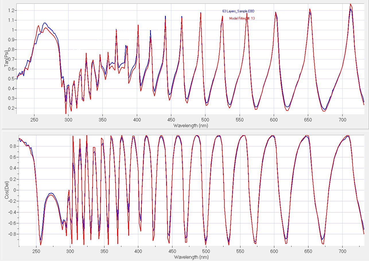
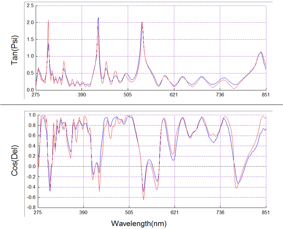
Spectroscopic Ellipsometer Application Example 1: Measured and Fitted graph for a total of 63 layers Oxide/Nitride film stack on a Silicon substrate:
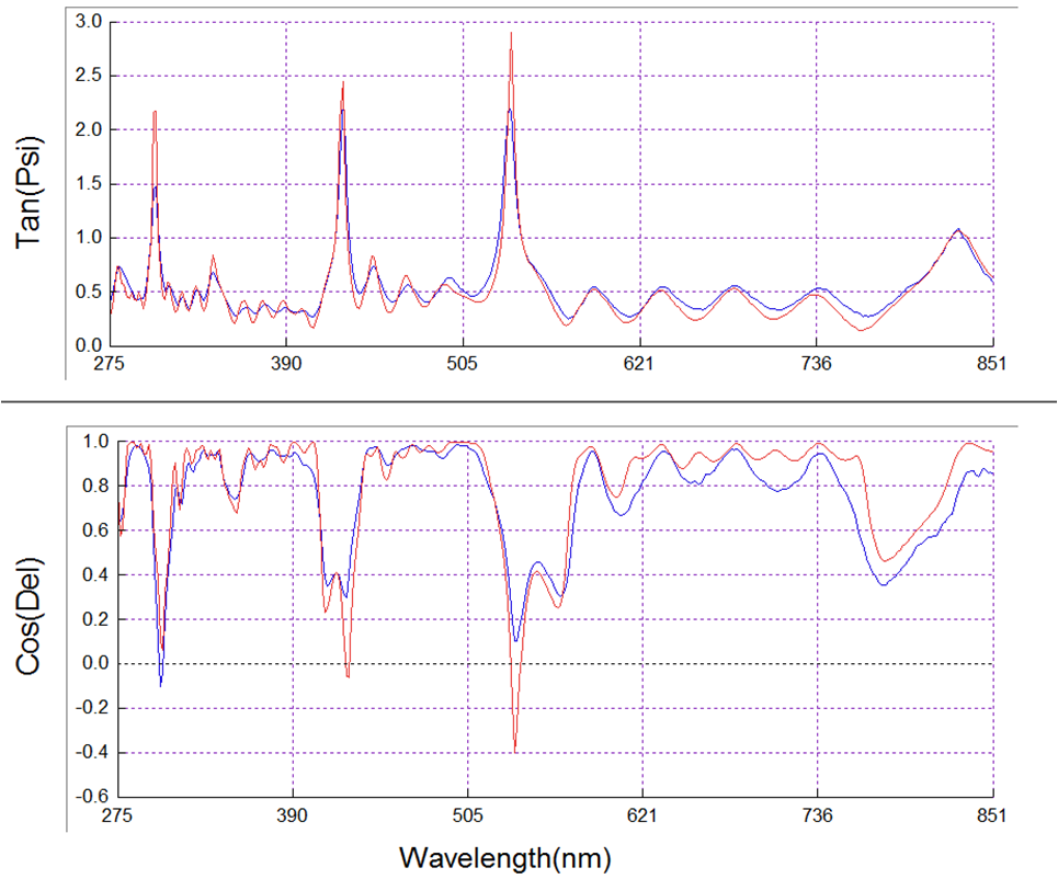
Spectroscopic Ellipsometry Application Example 2: Variable Angle Ellipsometer Measured Multiple Layer Stack
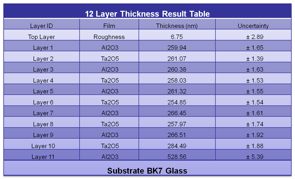
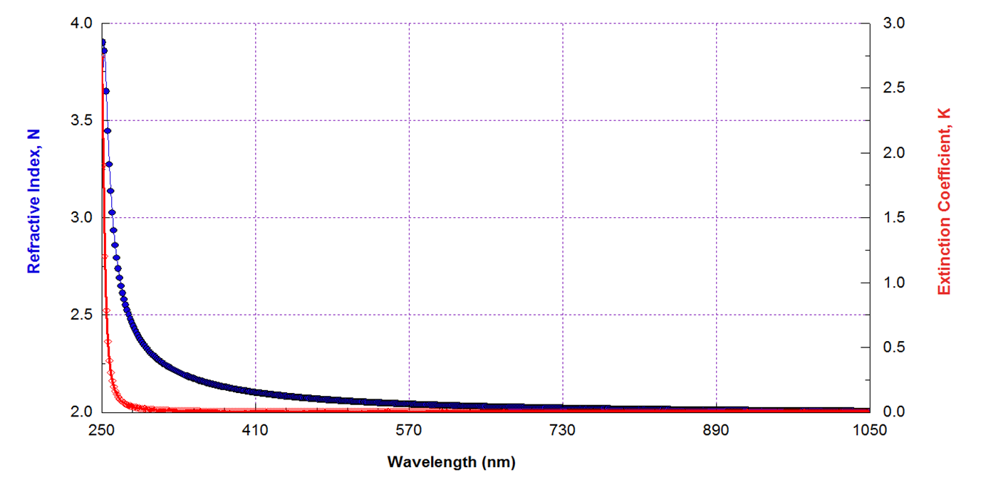
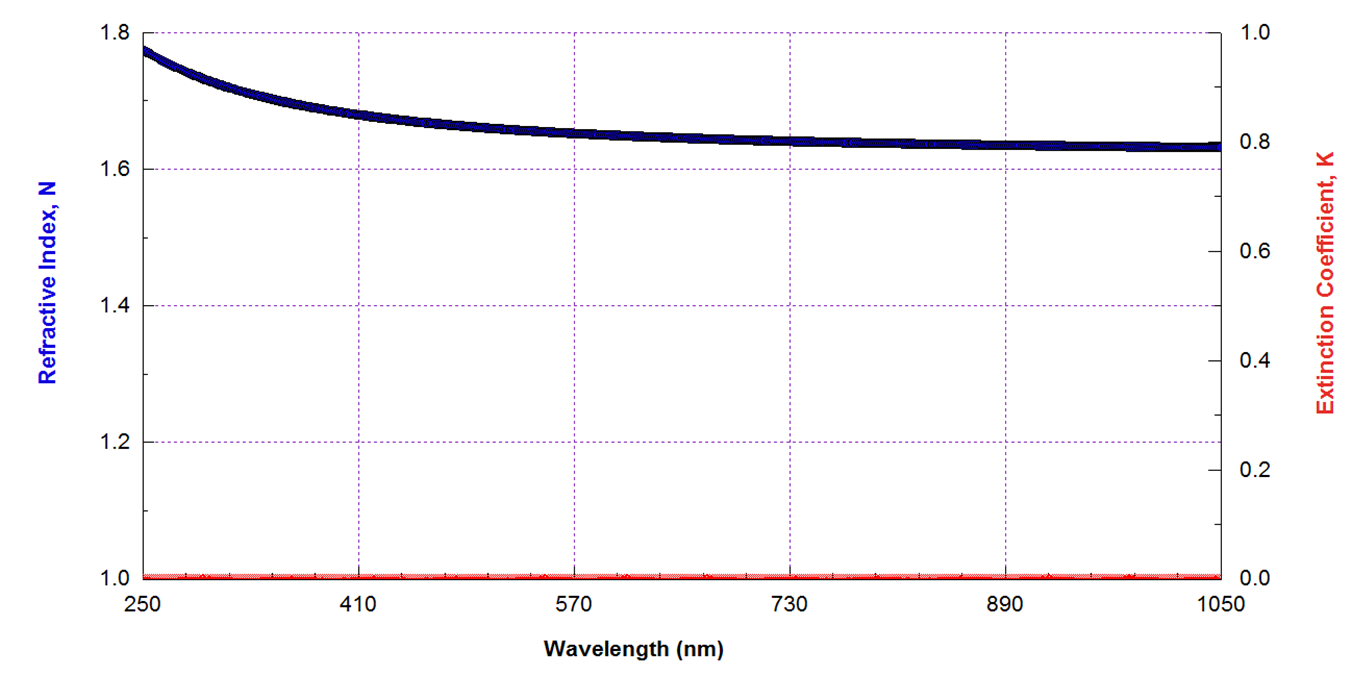
One sample with 11 Layers plus one surface roughness layer (total 12 layers in model) has been successfully measured with SE200BA tool. Ellipsometer raw data were collected at three different incident angles automatically, 65, 70 and 75 degree. All layers' thickness and their optical constants (refractive index and extinction coefficient) were obtained by fitting all data collected. This example shows variable angle measurement capability is essential for complicated layer stack applications.
Table Results for the sample analyzed with Spectroscopic Ellipsometer
Fitting Graphes for three different incident angles measured with Spectroscopic Ellipsometer SE200BA
65 Degree AOI Data Fitting (Blue curves are raw data and red curves are model data)
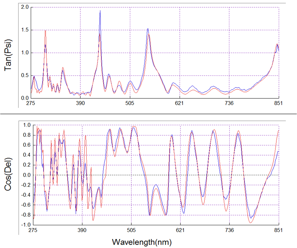
70 Degree AOI Fitting (Blue curves are raw data and red curves are model data)
75 Degree AOI Fitting (Blue curves are raw data and red curves are model data)
Measured Optical Contants for Ta2O5 Film In the Stack
Measured Optical Contants for Al2O3 Film In the Stack
Note:
- System configuration and Specifications subject to change without notice
- * Film property, surface quality and layer stack dependent
- Customized system available for special applications
- TFProbe is registered trademark of Angstrom Sun Technologies Inc.