
products categories
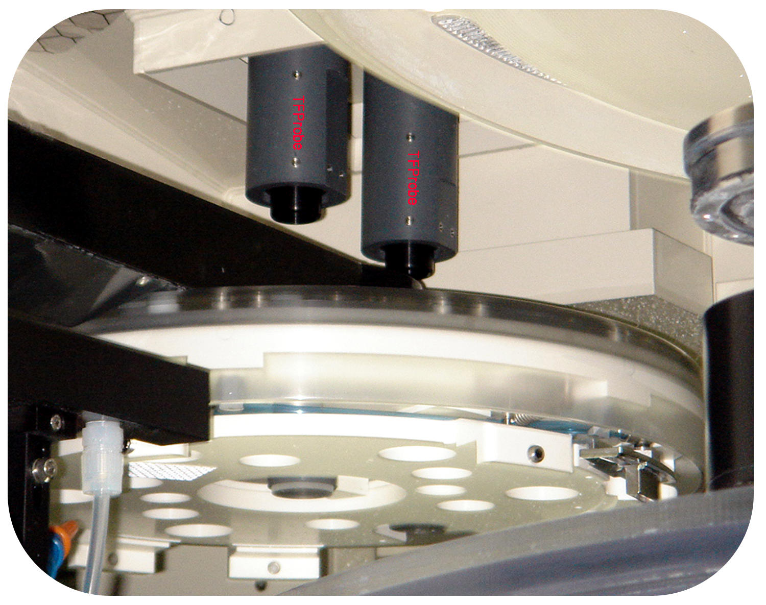
Chemical Mechanical Polishing/Planarization (CMP) is a process of smoothing surfaces with the combination of chemical and mechanical forces. It can be thought of as a hybrid of chemical etching and free abrasive polishing. Angstrom Sun Technologies Inc has implemented multiple channel in-situ spectroscopic reflectometers in such CMP processing system, plus one channel for pre-CMP. With such implementation, CMP processing can be well controlled by knowing inital thickness and before each sub-steps. By implementing multiple channels to monitor more than one location on the polishing wafer, processing uniformity information can be obtained which is also an impotant factors in CMP performance.
For patterned product wafers, Angstrom Sun Technologies inc developed Zonerage model with large spot measurement. Dielectrics inside probing area can be reliably characterized.
- Low cost
- Operate with Window based software
- Advanced optics with large spot design for best system performance
- Array based detector system to ensure fast measurement
- Uniquely designed light source for better intensity stability
- Real time or in-line Monitoring film thickness and Refractive Index up to 5 layers
- Multiple Channel/Multiple Sites Simultaneous Measurement
- System comes with comprehensive optical constants database and library
- Apply to many different type of substrates with different thickness
- RS232 Protocol for Host Control
- Auto log spectrum, thickness results and fitting graphs
- Advanced Global ZR model allows to extract local desired information from Large Spot Area Measurement over the patterned structure such as IMD, ILD1, ILD3 etc.
- One pre-CMP Channel for initial thickness measurement so tool can define the first step CMP time
- Two Channel for monitoing thickness after the first step CMP
- Two Channel for Monitoring thickness after the second Step CMP
- High Power DUV-Visible Light Source
- Communication Protocol between controller and Host Computer
- Flexible Fiber Optics for light beam delivery and detecting signal
- TFProbe 2.2 software for configuration, measurement and analysis
- Wavelength range: 400 to 1000 nm
- Spot Size: 20mm
- Wafer Size: 300mm
- Substrate Size: 300mm
- Measurable thickness range*: 20 nm to 10 µm
- Measurement Time: 2 ms minimum
- Accuracy*: better than 0.5% (comparing with ellipsometry results for Thermal Oxide sample by using the same optical constants)
- Repeatability*: < 1 Å (1 sigma from 50 thickness readings for 1500 Å Thermal SiO2 on Si Wafer)
- 1. More Channels can be added into the system
- 2. Wavelength range can be extended or expanded upon request
Note:
- System configuration listed above was customized
- * Specification is the film property, surface quality and layer stack dependent
- Almost every in-line tool is customized. Please contact us to discuss your application needs
- TFProbe is registered trademark of Angstrom Sun Technologies Inc.