products categories
Angstrom Sun Technologies Inc offers optical measurement and inspection systems for semiconductor and related industries. Its core products include wafer measurement systems, spectroscopic ellipsometers, thin film reflectometers, and microspectrophotometers.
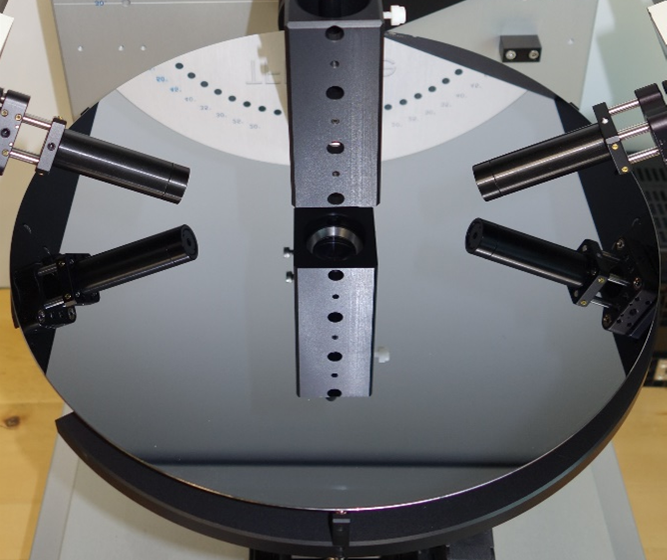
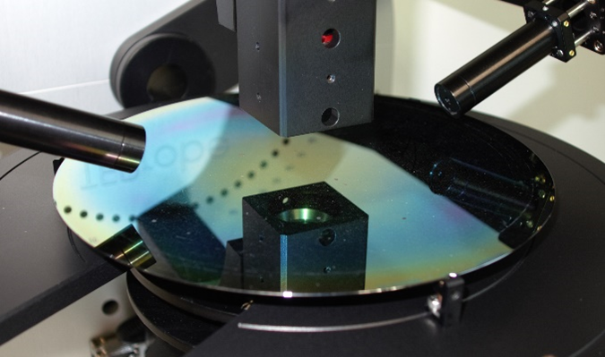
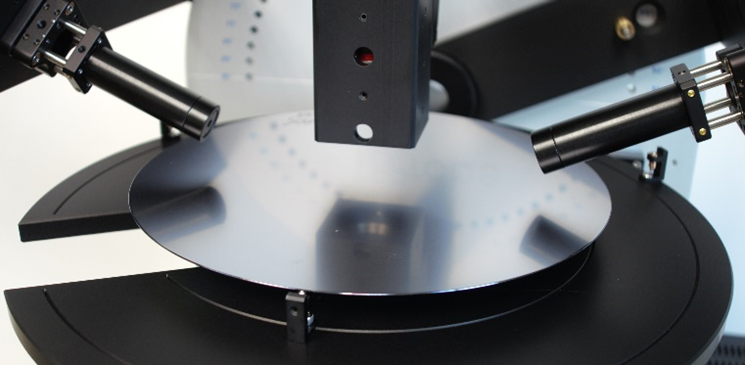
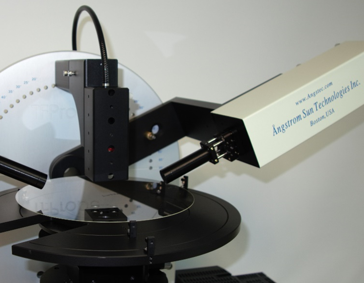
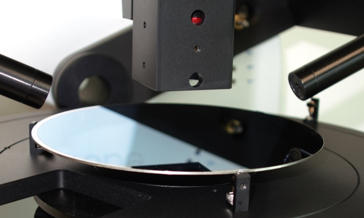
TFProbe wafer measurement systems, TFProbe WM series, measure wafer thickness, warp, bow, flatness, step/bump height, trench depth. TFProbe WM systems are based on confocal optical method with advantages of non-contact, non-destructive, long working distance, fast data acquisition, full mapping functions. Particularly, with integration with our thin film measurement technique, a total solution for thickness measurement covers from a few angstroms to several millimeters. Another key feature is that all our tools are upgradable in future.
TFProbe software works under both Windows 32-Bit and 64-bit OS window systems. It can be delivered with one function, several functions or full functions to cover different applications. It has also several access level such as engineer mode, operator mode and service mode. Furthermore, Angstrom Sun Tech provides professional support, lifetime free upgrade on software. Customized functions can also be integrated into it. TFProbe WM is available in manual, semiautomatic, and cassette loading fully automatic configurations for wafer sizes up to 300 mm.
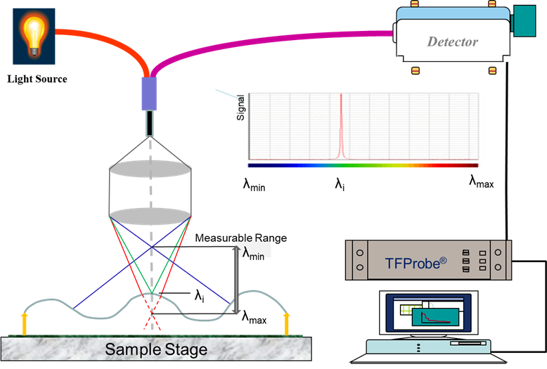
Measurement Principle:
- Great performance at low cost
- Modular design, easy to set up, virtually no maintenance required
- Easy to operate with Window based software
- Non-contact, non-destructive, ultra-long working distance
- Compact, Advanced optics design for best system performance
- Long Lifetime light Source (over 8 years)
- Array based detector system to ensure fast measurement
- Application types: wafer warp, wafer bow, wafer thickness, wafer thickness variation (TTV), glass wafer thickness, trench depth, bump height, air gaps sandwiched between two transparent plates and more,
- Capable to be used for real time or in-line monitoring
- System comes with comprehensive optical constants database and library
- Integrable with spectroscopic ellipsometer or reflectometer for thin film measurements on all different type of wafers
- Apply to many different types and sizes of substrates
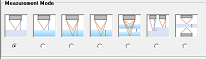
- TFProbe software allows to various scanning patterns, linear, square, non-square, polar, user-defined….
- 2D and 3D output graphics and user-friendly data management interface
- Model: TFProbe WMxxx
- Light Source: over 8 years Long Lifetime Source
- Spectrometer: 2048-pixel detector
- Motorized Stage: 2” to 12” range selectable
- Precision Z stage with tilting adjustment
- Three-point ball support for wafers to free standing
- Sample Plate: up to 300mm size with pins for various sizes of wafers
- Communication: USB
- Computer: Intel i3 processor, 8GB ram and 500GB Hard Drive with Keyboard and Mouse
- Monitor: 22” LCD Monitor
- Software: TFProbe 3.3
- Power input: World-wide, universal 110– 240 VAC /50-60Hz, 1.5 A
Note: system will be configured per quote to meet applications.
|
Item |
Specs |
|
Wafer Size |
2/4/6/8/12” or customized |
|
Working Distance |
~30mm |
|
Stage |
Rho-Theta for up to 12” Wafer or customized |
|
Measurable Range |
5mm |
|
Precision |
0.1µm |
|
Data Acquisition Rate |
1ms |
|
Measurement Spot Size |
500um |
|
Software |
TFProbe 3.3 |
|
Computer |
Intel i3 8GB RAM, 500GB hard drive |
|
Monitor |
22” |
|
Main Unit Dimension |
20(W)x22(D)x20”(H), without ellipsometer integration |
|
Main Unit Weight |
~150 lbs. |
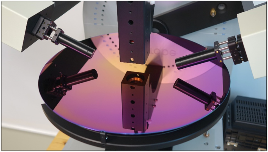
- Dual heads for non-transparent substrate property measurement
- Small spot for measuring trench depth
- In-Situ or in-line Integration and Processing Monitoring
- Multiple Heads for simultaneously measurement at multiple locations for step or bump heights
- Mapping uniformity for non regular wafer size samples
- Simple, low cost one spot measurement setup without motorized stages
- Flatness/Warpage /Displacement for non-transparent Wafers
- Flatness/Warpage /Displacement for transparent Wafers on its top surface
- Flatness/Warpage /Displacement for transparent Wafers on its bottom surface
- Thickness of transparent Wafers
- Gap Thickness between two transparent wafers/Layers
- Step Height with two sensor heads
- Non-transparent wafer thickness with two sensor heads
- One head for transparent wafer (Glass, SiC, Sapphire, Quartz, PET sheet….) thickness
- One head for wafer displacement variation, Bow, warp measurements
- One head for step/bump height, trench depth measurement via motorized stage scanning
- One head for gap thickness measurement between two glass plates
- Two heads for non-transparent wafer or plate thickness measurement (Si, InP, GaAs, Ge…)
- Two heads for step/bump/trench depth measurement without motorized stage
- In-Situ or in-line Integration and Processing Monitoring
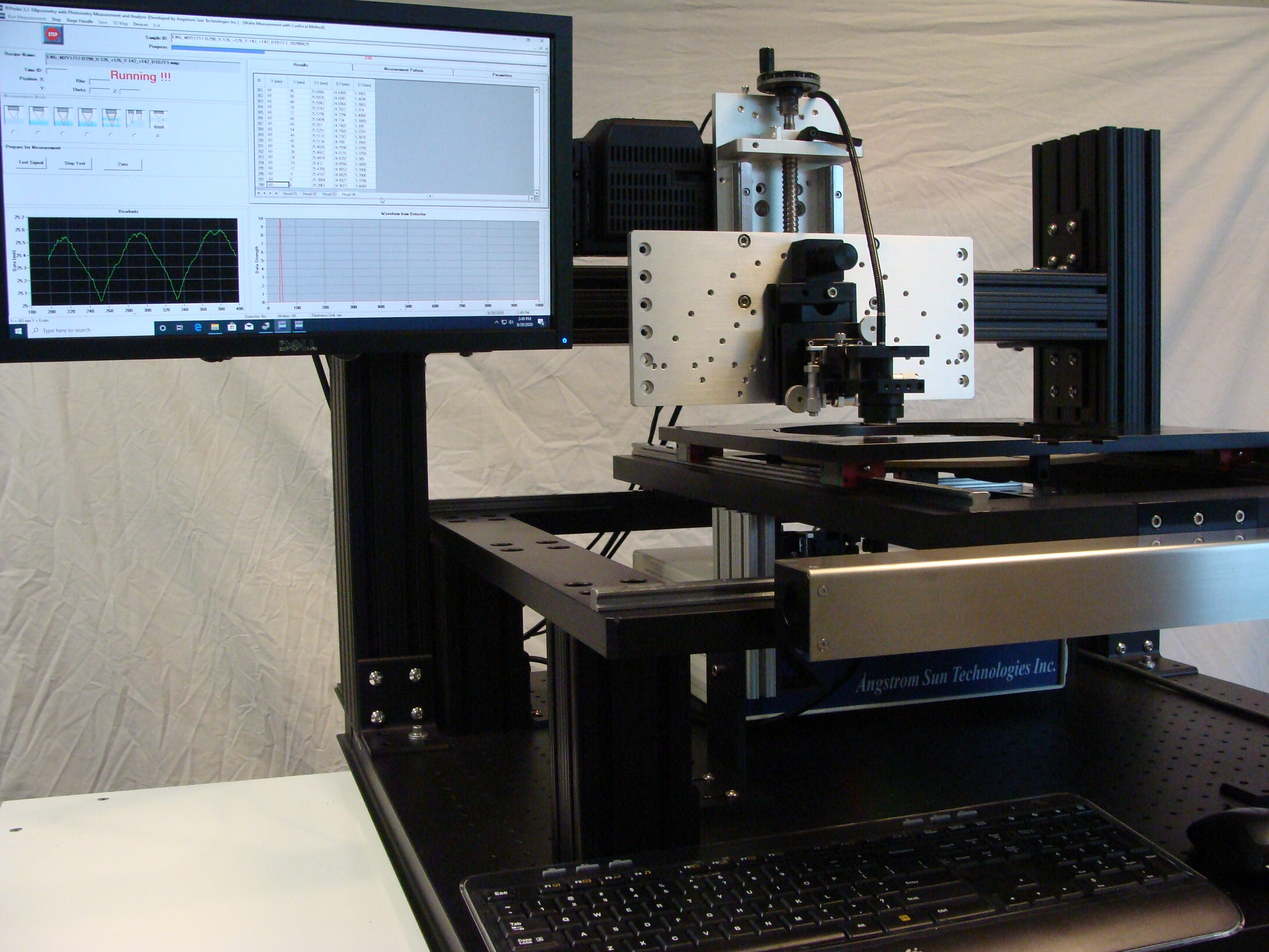
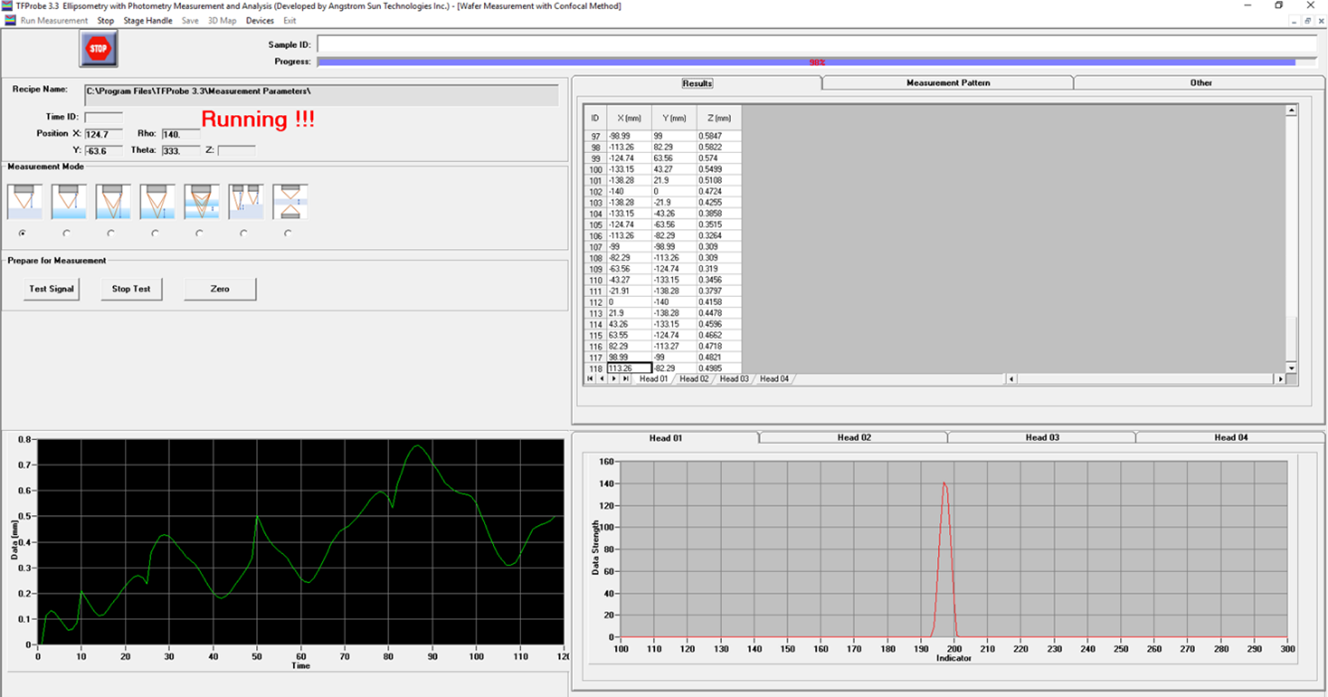
Real Time Running Display:
1. 300mm Silicon Wafers:
2. 200mm silicon Wafer with thin films on it
3. Unpolished 200mm Silicon Wafers:
4. 200mm Glass Wafers
5. 6” Metal Wafers:
Output Examples
1. Step Height and Profile of Surface Features


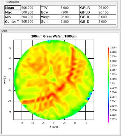
2. 200mm Glass Wafers (500um Thickness)
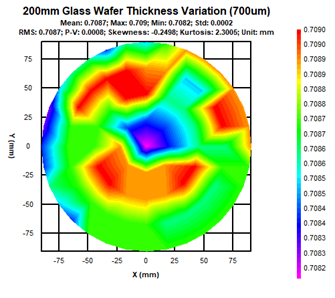
3. 200mm Glass Wafers (700um Thickness)
Note:
Dual sensor setup with 300x300mm measurement capability: