
products categories
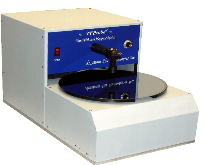
When you need processed thin film uniformity information, our SRM series mapping tool is for your consideration. Spectroscopic Reflectometer Mapping (SRM) series tool is based reflectometry technique and with the same working principle as spectroscopic reflectometer. SRM series allow you to map film thickness and refractive index up to 5 layers. No need to worry about complicated equipment since the SRM tool is easy to setup and operate. It uses Windows based software. Mapping up to 200mm and 300mm wafer sizes are our standard configuration. For wavelength range coverage, both DUV-Visible (SRM100) and Visible range (SRM300) are available. Other wavelength ranges, mapping size and mapping geometry can be customized upon request. Advanced software allows user to generate various types of mapping patterns such as linear, polar, square or even arbitrary coordinates. The array-based detector system ensures the fastest film thickness measurement. With its advanced optics and rugged design, you can always be sure to get the best system performance.
- Easy to set up and operate with Window based software
- Various types of geometry substrate up to 300mm in diameter
- Various types of mapping pattern such as linear, polar, square or arbitrary coordinates
- Advanced optics and rugged design for best system performance
- Array based detector system to ensure fast measurement
- Map film thickness and Refractive Index up to 5 layers
- System comes with comprehensive optical constants database and library
- Include commonly used recipes
- Advanced TFProbe Software allows user to use either NK table, dispersion or effective media approximation (EMA) for each individual film.
- Upgradeable to MSP (Microspectrophotometer) mapping system with pattern recognition, or Large Spot for mapping over patterned or featured structure
- Apply to many different types of substrates with different thickness
- 2D and 3D output graphics and user-friendly data management interface with statistical results
- Output mapped resutls in csv file format
- Long lifetime lamps included with system
- All USB communications and PC controlled
|
Model |
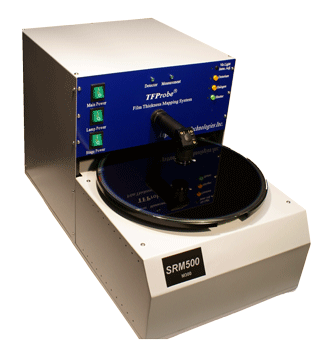
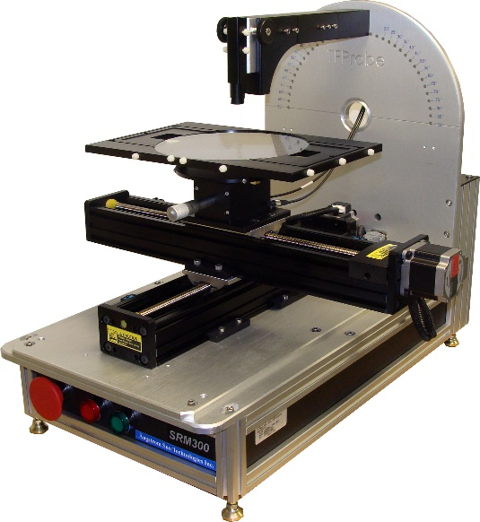
SRM100 |
SRM300 |
SRM500 |
|
Detector Type |
CCD or CMOS Array |
CCD or CMOS Array |
CCD or CMOS and InGaAs Array |
|
Wavelength Range (nm) |
190 to 1100 |
370 to 1100 |
190-1700 |
|
Wavelength Resolution |
0.01 -3nm |
0.01 -3nm |
0.01 to 3nm |
|
Measurable Thickness Range |
5nm to 50 µm |
20nm to 1000 µm |
5nm to 1000 µm |
|
Thickness Precision |
< 1Å (1 sigma from 50 thickness readings for 1500Å Thermal SiO2 on Si Wafer) |
||
|
Thickness Accuracy |
better than 0.5% (comparing with ellipsometry results for Thermal Oxide sample by using the same optical constants) |
||
|
Stage |
Black Anodized Vacuum Chuck, typical Rho-Theta for compact size, 200mm, 300mm or customized size per request |
||
|
Working Distance |
~ 20mm (from Wafer Surface) |
||
|
Measurement Time |
0.1 milliseconds to 10s, user definable |
||
|
User Definable |
Wavelength range, wavelength points, integration time, spectra average numbers, smooth factors |
||
|
Software |
TFProbe 2.4 or TFProbe 3.3 |
||
|
Communication |
USB |
||
|
Operating System |
Both 32bit and 64 Bit, Win XP, 7, 8, 10 |
||
|
Computer Requirement |
Intel i3 or above with minimum 500 MB space, 4GB RAM |
||
|
Power Input |
World-wide, universal 110– 240 VAC /50-60Hz, 1.5 A |
||
|
Light Source |
Deuterium + Tungsten Halogen |
Tungsten Halogen |
Deuterium + Tungsten Halogen |
|
Light Source Intensity |
Adjustable |
Adjustable |
Adjustable |
|
Lifetime of Lamp(s) |
4000 hrs. |
10000 hrs. |
4000 hrs. |
- Power: 110– 240 VAC /50-60Hz, 3 A
- Dimension: 14”(W) x 20”(D) x 14”(H)
- Weight: 100 lbs
- Warranty: One year labor and parts
- System will be configured within above specified wavelength ranges per quote to meet specific applications
Example Setup 1 (SRM300-M300):
Example Setup 2 (SRM300-MX300Y200):
- Wavelength Extension to DUV or NIR Range
- Customized mapping size: Available
- Large Spot Accessories for featured structure measurement
- Small spot accessories for highly non uniform samples
- SRM series could be configured with different platforms per applications' need and some special functions or options
- Semiconductor fabrication (PR, Oxide, Nitride..)
- Liquid crystal display (ITO, PR, Cell gap…..)
- Biological films and materials
- Optical coatings, TiO2, SiO2, Ta2O5…..
- Semiconductor compounds
- Functional films in MEMS/MOEMS
- Amorphous, nano and crystalline Si
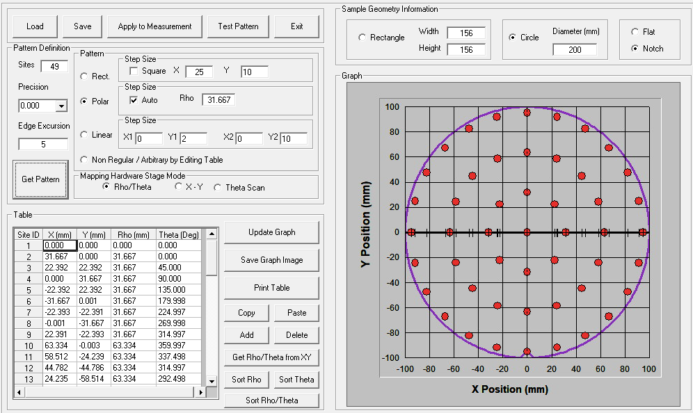
Mapping Pattern Difinition Interface:
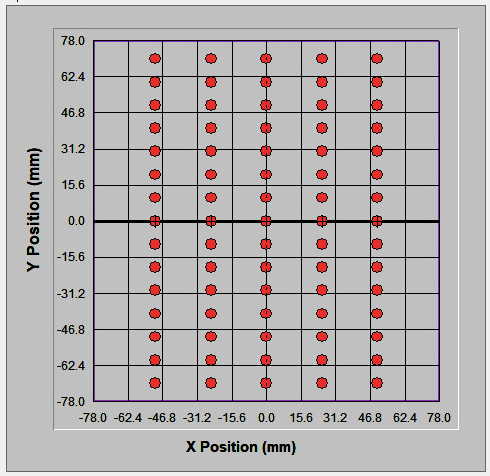
User can define mapping pattern with polar, square, non-square, linear or with arbitrary input. Edge exclusion and precision can be defined by user. Software also allows user to copy from other formats and paste into TFProbe table to generate the same pattern. Following example shows a 49-pts pattern defined with equal spacing, 5mm edge exclusion and 3 decimal precision for 200mm wafer:
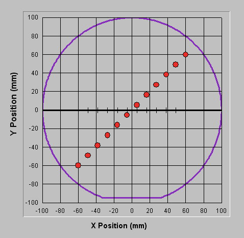
Linear Pattern Example:
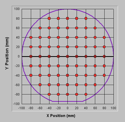
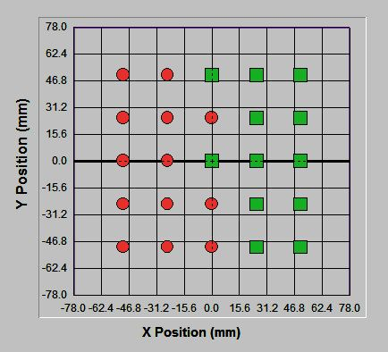
Square pattern:
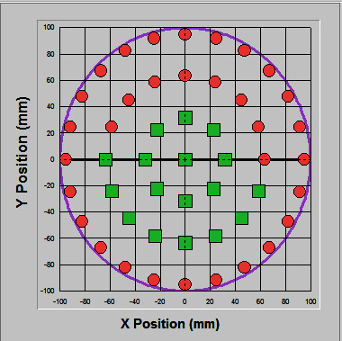
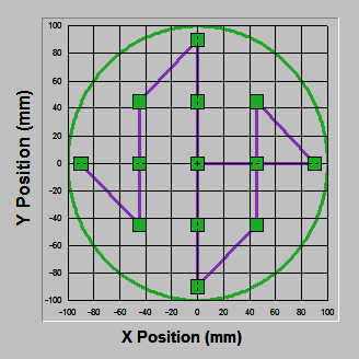
A Non-square pattern example:
After pattern is defined, user can test it and optimize it based on travel distance and speed. Here are some examples:
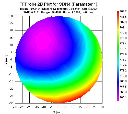
- 2D thicknesses plot for Nitride layer in a three layer stack (Nitride-Oxide-Nitride on Glass)
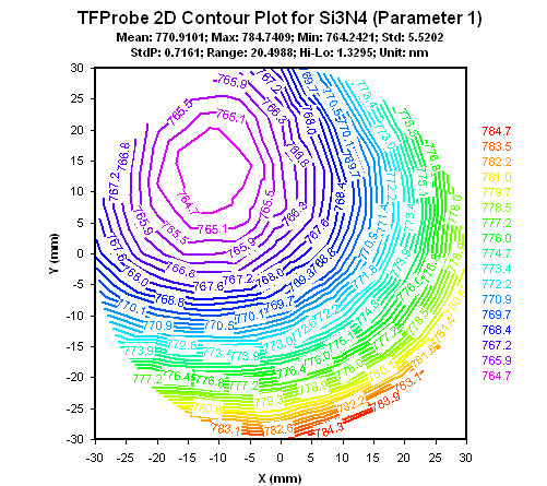
- 2D contour plot for Nitride layer in a three layer stack (Nitride-Oxide-Nitride on Glass)
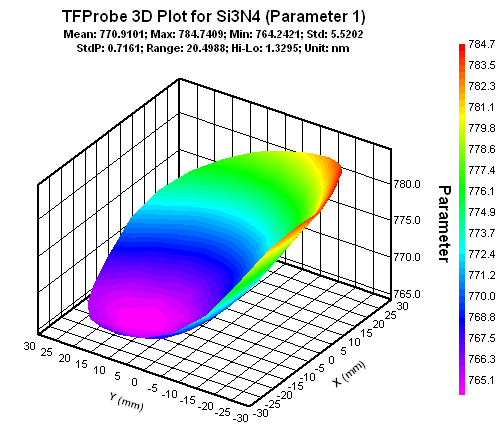
- 3D plot for Nitride layer in a three layer stack (Nitride-Oxide-Nitride on Glass
Note:
- System configuration and Specifications subject to change without notice
- * Film property, surface quality and layer stack dependent
- Customized system available for special applications
- TFProbe is registered trademark of Angstrom Sun Technologies Inc.